R&D outcome and application examples utilizing SPS:
Spark Plasma Sintering (SPS) technologies are being rapidly permeated into institutes and industries these days. Not only universities or industries in Japan, those in overseas countries are interested in SPS effect. The major interest which many industries are showing is if it is applicable not only to R&D in their laboratories but also to actual production processes. As the matter of fact, numbers of SPS applications are being promoted in electric, automotive, electronic, dies & molds, cutting tools, bio-energy, aerospace and other industries.
Application examples:
- Fine ceramics / cermet
- Metal, Intermetallic compound and alloys
- Electronic materials: Target materials, Thermoelectric element, Thermal conductivity element, Piezo electric devices, Ferroelectrics, Magnetic bodies, etc.
- Advanced composite and Composite materials: Carbon nano-tube(CNT), Carbon nano-fiber(CNF)
- Composite technologies: Solid phase diffusion bonding, Sinter bonding, Sheet bonding and Graded bonding etc.
- Nano-phase materials and Nano-structure materials
- Porous materials
- Hard materials
- Dies and Molds materials: Non-spherical glass molds for digital camera lens, Die-cast dies, Plastic molds with flow channel for cooling fluid, Press dies and molds.
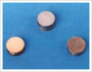
- Corrosion resistance and wear resistance materials: Diamond tools, WC alloy, CBN, Mounted wheel, Cutting blade, Blasting nozzle,
- Biomaterials, Functional materials
R&D application examples of our team:
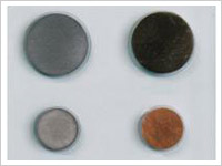
Target materials
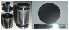
High purity SiC (without binder)
High density SiC (relative density:99%)
Conductive SiC
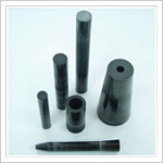
Wear resistant ceramic
parts
(Near net shape forming)
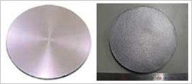
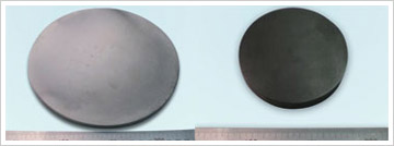
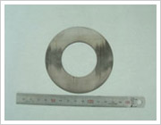
Large sized ceramic
(300mm dia.)
Advanced Composite material
(Carbon nano-tume)
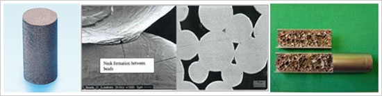
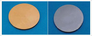
High density sintering materials:
Left: High purity alumina Right: WC without binder
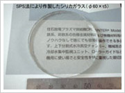
Silica glass
Thermo electric material
Diamond composite material
(Diamond tool)
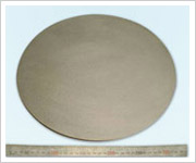
Porous materials
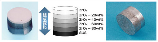
Functionally graded materials: Right: Porous + Refined solid
Left: Zirconia + Stainless Steel: (by grain size blending)
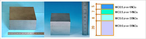
Functionally graded material WC + Co
Left: 100mm x 100mm x 40mm Right: 40mm x 40mm x 40mm
WC + Co
Diamond cutting blade
High density sintering of “difficult to sinter” materials
Left: TiN Right: CrN